


Department of Computer and Communication Engineering
College of Electrical & Computer Engineering
Communication Circuits & System Design Lab. [Professor Kyoung-Rok Jo]
Professor

- Kyoung rok cho (E8-10-306 / 043-261-2368)
- Lab : Communication Circuits and System Design (CCNS) / http://ccns.cbnu.ac.kr
- h.D, The University of Tokyo, 1992
- 1979~1986: Chief Engineer LG Co. Ltd., Korea TV Research Center
- 1999, 2005: Visiting Professor at Oregon State University
- Since 2010: Director of IDEC at CBNU
- Current Research Areas: High Speed, Low Power Circuits(small size circuit), Ad-hoc Embedded Controller Design, Gbps Interface Circuit Design for LCD Display IC, Communication System Chip Design(OFDM based), Emerging Circuit Design
- Bachelor’s degree in Kyeongbuk National University, Master’s degree & Doctor's degree in University of Tokyo, Japan
- 1979~86 a senior researcher of LG TV research institute
- 1992~ currently a professor of information communication engineering department of electronic information college in Chungbuk National University
- 2007 a strategic, technical and advisory committee member in the Ministry of Science and Technology
- 2010 ~ currently IDEC Chungbuk National University community centre
- 2013 awarded Minister prize of Ministry of Trade, Industry and Energy
Research Area (CCNS LAB)
- Low Power and High Speed Circuits Design
- Ad-hoc Embedded Micro Controller Design
- Communication System Chip Design (OFDM based)
- LVDS, RSDS, MIPI, Display Interface Circuits
- CMOS Image Sensors
- Memristor [4th circuit element] modeling and application circuits
Research Project (in progress)
- A technical development of a general-purpose, powerless RF remote control
- An advanced track of electric power/IT convergence for Zero-Sum power consumption
- A sensor circuit research on retina photodiode based on CMOS for an artificial retina
Research Project (the recent three years)
- V-by one High Speed Interface Circuits - The Ministry of Knowledge Economy
- SSD NAND Flash Memory Controller Design – SK Hynix
- Memristor-MOS Imaging System - Ministry of Education and Science Technology(MEST)
- CMOS Image Sensor for camera - Ministry of Education and Science Technology(MEST)
Prototype picture related the development
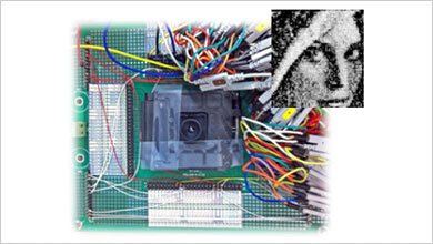 CMOS image sensor chip
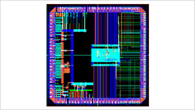 MIPI interface chip
Lab (CCNS LAB.)
- Location : Room #309, building E8-10(508 dong)
- Contact : 043-261-3573
- An academic advisor : Gyeong-Rok Jo